Advanced Design & Assembly Services
Backend process services for your needs
in Semiconductor and Photonics.
Argotech offers the entire back-end assembly process chain from wafer level assembly to full optical assembly of customised semiconductor packaging solution. This enables prototyping and pilot production with the potential to rapidly scale up to volume production.
Our R&D teams can assist with feasibility studies, product design, prototyping, product qualification and process modifications.
Argotech is exclusively a SERVICES provider with inhouse capacity of various semiconductor packaging platforms and a wide range of R&D services but does not market its own products.
The SERVICES are divided into three main groups:
- Manufacturing services
- R&D services
- Testing services
Our key features and benefits for our partners include:
- Packaging capabilities for multispectral applications (200nm – 20µm)
- Operating with cutting-edge technologies while working for leaders in the industry
- Providing solutions combining Optical, Electronic and Mechanical design and technologies.
- Experienced engineering teams with sustainable equipment investments
- High quality standards
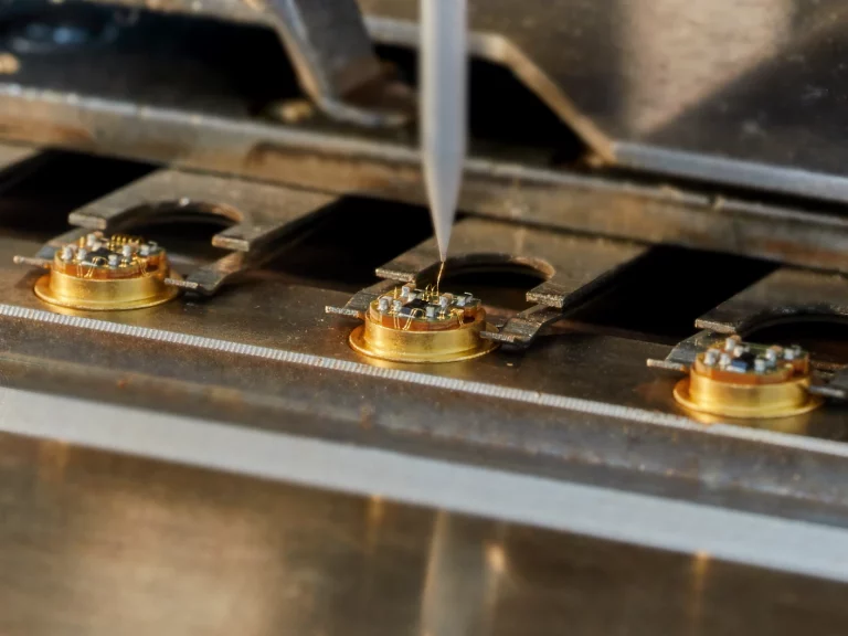
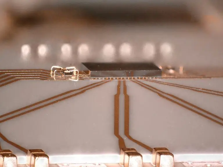
Manufacturing services
Volume:
Flexible production volume capacities from single piece to higher volume batches.
Complexity:
We offer optional assembly process complexity from single chip packaging to the complex device packaging, with the possibility to use any part of the processes or the entire assembly line.
Contract models:
- CM – contract manufacturing
- OEM – original equipment manufacturing
- ODM – original design manufacturing
- Die-Attach
- Wire bonding
- Optical coupling / Active alignment
- Solder ball jetting and related soldering processes
- Testing and Burn-in
- Inter-process verification – PBI
- Hermetic sealing and packaging
- Supporting processes – dicing, characterization, laser marking
R&D services
Whatever stage your concept readiness is at, we can start with a feasibility study to prove the concept and recommend further steps to achieve your best parameters.
Our experienced team of development engineers can support partners with bridging the gaps in the packaging aspect.
In addition we provide valuable feedback to front-end chip designers so that their components can be further efficiently integrated into semiconductor packages.
We provide the following outputs based on project readiness level:
- Simulations – thermal, high frequency, optical path, electrical
- Feasibility study, proof of concept
- Design – mechanical and optical
- Prototype build – evaluation and qualification
- Assembly process development
- Sample batch verification
- Public funded projects
- Long-term R&D contracts
Do you need more information?
We are ready to assist you. Contact us directly here and give us a brief description of your project.
We will get back to you as soon as possible.
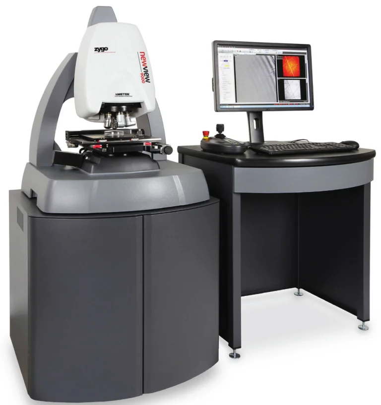
Testing services
Standard testing services according to your needs or industry standards using our testing facilities, specialized systems and devices.
- Component characterization
- Qualification according to standards
- Burn-in, accelerated ageing life tests
- Environmental testing
- Selected standard compliance testing
- Mechanical tests
- Surface analysis